false
0001828805
0001828805
2024-01-30
2024-01-30
iso4217:USD
xbrli:shares
iso4217:USD
xbrli:shares
UNITED STATES
SECURITIES AND EXCHANGE COMMISSION
Washington, D.C. 20549
FORM 8-K
CURRENT REPORT
Pursuant to Section 13 or 15(d) of the Securities
Exchange Act of 1934
Date of Report
(Date of earliest event reported): January 30,
2024
Aeluma, Inc.
(Exact name of registrant as specified in its
charter)
| Delaware |
|
000-56218 |
|
85-2807351 |
|
(State or other jurisdiction
of incorporation) |
|
(Commission File Number) |
|
(IRS Employer
Identification No.) |
|
27 Castilian Drive
Goleta, California |
|
93117 |
| (Address of principal executive offices) |
|
(Zip Code) |
805-351-2707
(Registrant’s telephone number, including
area code)
Check the appropriate box below if the Form 8-K
filing is intended to simultaneously satisfy the filing obligation of the registrant under any of the following provisions:
| ☐ |
Written communications pursuant to Rule 425 under the Securities Act (17 CFR 230.425) |
| ☐ |
Soliciting material pursuant to Rule 14a-12 under the Exchange Act (17 CFR 240.14a-12) |
| ☐ |
Pre-commencement communications pursuant to Rule 14d-2(b) under the Exchange Act (17 CFR 240.14d-2(b)) |
| ☐ |
Pre-commencement communications pursuant to Rule 13e-4(c) under the Exchange Act (17 CFR 240.13e-4(c)) |
Securities registered pursuant to Section 12(b) of the Act: none.
Indicate by check mark whether the registrant
is an emerging growth company as defined in Rule 405 of the Securities Act of 1933 (§230.405 of this chapter) or Rule 12b-2 of the
Securities Exchange Act of 1934 (§240.12b-2 of this chapter).
Emerging growth company
☒
If an emerging growth company, indicate by check
mark if the registrant has elected not to use the extended transition period for complying with any new or revised financial accounting
standards provided pursuant to Section 13(a) of the Exchange Act.
Item 8.01 Other Events.
We are filing
this report to disclose a Company PowerPoint presentation, a Company flier, and three product offering brochures. The presentation,
flier, and brochures are all furnished as exhibits to this Current Report on Form 8-K.
Neither this report nor the exhibits attached
hereto constitute an offer to sell, or the solicitation of an offer to buy our securities, nor shall there be any sale of our securities
in any state or jurisdiction in which such offer, solicitation or sale would be unlawful prior to the registration or qualification under
the securities laws of any such state or jurisdiction.
Item 9.01 Financial Statements and Exhibits.
(d)
Exhibits.
SIGNATURE
Pursuant to the requirements of the Securities
Exchange Act of 1934, the registrant has duly caused this report to be signed on its behalf by the undersigned hereunto duly authorized.
| |
AELUMA, INC. |
| |
|
|
| Date: January 30, 2024 |
By: |
/s/ Jonathan Klamkin |
| |
|
Jonathan Klamkin |
| |
|
President, Chief Executive Officer and Director |
2
Exhibit
99.1
Sen s i ng Rei ma g i n e d TM L a rge - W a fer Het erog e neously In t egr a t e d InG a As Pho t ode t ec tor Sensors Matthew Dummer , Jonathan Klamkin, Bei Shi, Bowen Song, Simone S. Brunelli, Michael McGivney, Douglas Oakley, Daniel Renner P a per 1 2 88 0 - 18 J an u a r y 30, 2 0 24 © Aelu m a , Inc. All R i g ht s R e serve d .

Outline © Aelu m a , Inc. All R i g ht s R e serve d . ● I ntrodu c tion to Aeluma ● Background on InGaAs detectors and scaling limitations ● Aeluma’s scalable large - diameter wafer platform ● D e te ct o r array p e rf o rma nce re s ults ● C o mparison to o ther de te ct o r te c h nologi e s ● Summary of product and technology offerings ● Conclusions

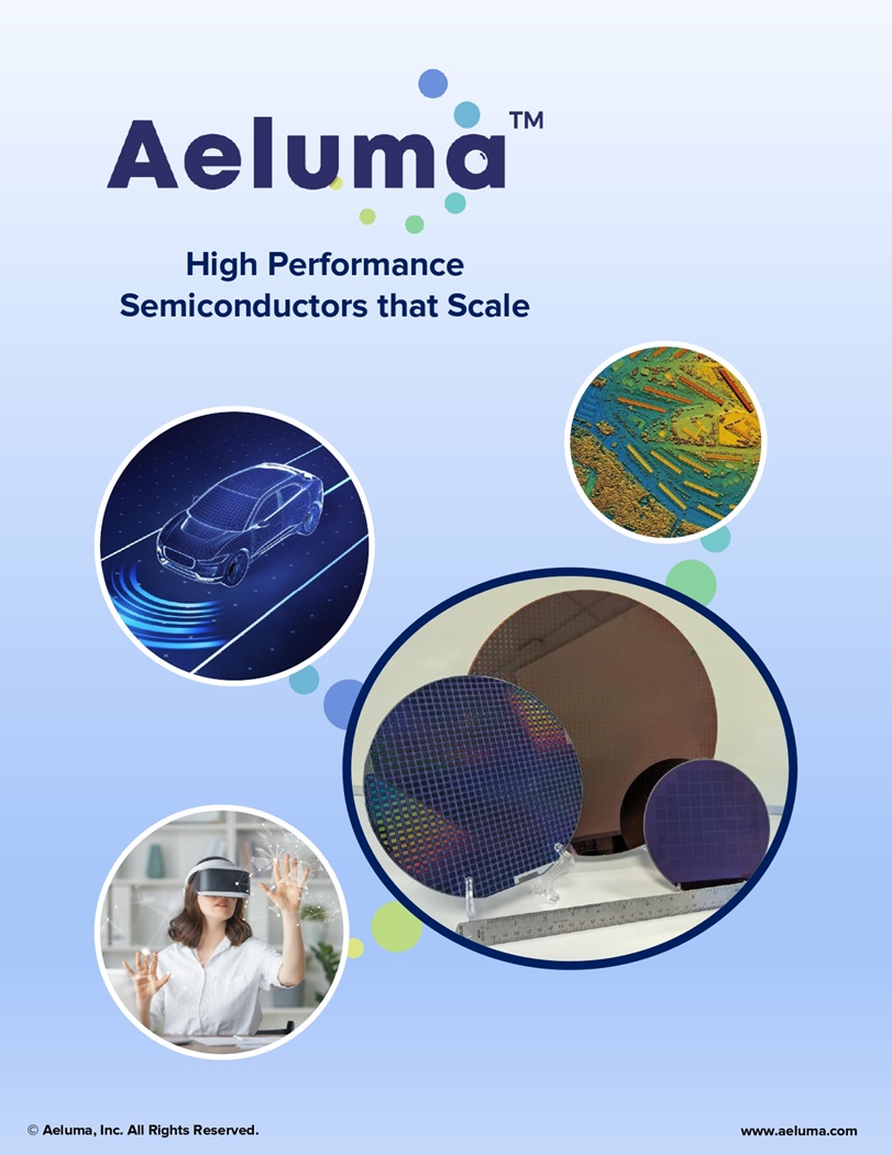
© Aelu m a , Inc. All R i g ht s R e serve d . At a Glance Aeluma, Inc. (O T C Q B : AL M U) A transformative semiconductor chip company High P e rf o rma nce S e mic o nduct o rs that Scale Headquarters : Goleta/Santa Barbara, California Ma rk e t s : Au t omot i v e LiDAR, Mob i l e, AR/VR, Communication, Defense & Aerospace, AI Te a m : ~15 people Ex p er t i s e : C ompound se mi c on d uct o r s , he t eroep i t a x y , photon i c i n t e gra t e d circ u i t s , s i l i c on photon i c s, l ase rs, d e t ectors, volume ma nu fact u r i ng I n t e l l ect ua l Pro p e r t y : ~25 i ss u e d a nd pen d i ng pat en t s, t rad e secr e t s 3

Background on InGaAs Detectors High Performance Detectors for Active and Passive Imaging © Aelu m a , Inc. All R i g ht s R e serve d . 4 InGaAs: Indium Gallium Arsenide; LiDAR: Light detection and ranging; FPA: Focal plane array. Note: Outcomes cannot be guaranteed. Sources of images: https://www.flir.com/support/products/swir - ingaas - fpa/; https://www.bhphotovideo.com; https:// www.wardsauto.com/vehicles/lidar - house - battery - production - volvo - s - sights; https://ouster.com/blog/mhttps://www.foresightauto.com/thermal - cameras - solve - autonomous - trucks - dust - problem/ake - intersections - sa fer - trb/; https:// www.deltaquad.com/vtol - drones/inspect/; www.digikey.com Be h i n d t h e “ E y e” Representative commercial InGaAs FPA for L i DA R a nd i m a g i ng a pp li c a t i ons I s s ue s p r e v e n t ing b r o a d m a r ke t a d o p t ion • S c a le : I ncub m b e n t I nGaAs i s speciali zed • Cost : Price for detector array is too high A elu m a ’s t e c hno l o g y se e k s t o a dd r e s s t he s e c h a l l e n g e s w i t h s c a l a b le , c o s t - e ffec t iv e m a nuf a c t u r in g . Perform a nce th at s c ales Automotive LiDAR Infrared Imaging

The Aeluma Approach to Photonics Manufacturing High Performance Technology with Large - Diameter Wafer Manufacturing © Aelu m a , Inc. All R i g ht s R e serve d . 5 In P : In d i u m P h o s p h i d e ; Source of image: https:// www.flir.com/support/products/swir - ingaas - fpa/; Note: Outcomes cannot be guaranteed. I n P subs t ra t e si z es I nG a A s F P A M a nu f a c t ur e d on InP substrates 4 in c h 3 in c h 8 in c h Silicon substrate sizes Lea p i ng from I nP t o S ili c o n 12 i n ch

Conventional manufacturing of I n G aA s ph oto d etect or a r r ays arrays with Si l i c on m an u fac t u ri n g Highly automated and ability to produce many arrays per wafer 10X lower manufacturing cost for mass market applications 1 6 X w a fer a re a Movi ng f r om 3 - i nch t o 12 - i nc h w af e rs Non - scalable, manual and low throughput Note: Outcomes cannot be guaranteed. © Aelu m a , Inc. All R i g ht s R e serve d . Aeluma’s Technology Breakthrough Scalable, Cost - Effective Manufacturing Enabled by Cutting - Edge Intellectual Property Aeluma high - performance InGaAs photodetector 6

Aeluma’s Cost - Effective Scalable Manufacturing Large - Diameter Wafer Capability ● Commercial 12 - inch state - of - the - art deposition tool ● Set up for cassette (FOUP) loading production ● One of only a few such tools worldwide ● Extensive patent protection and trade secrets © Aelu m a , Inc. All R i g ht s R e serve d . 23

Aeluma’s Cost - Effective Scalable Manufacturing Large - Diameter Wafer Capability Phot olum i n e s ce n c e Ma p p i ng Me a su re m e n t s 8 - i n ch Wafer M ap O ver l aid Scan s Excellent Uniformity Across Wafer InP - o n - Si l i c on W a fer © Aelu m a , Inc. All R i g ht s R e serve d . 23

Wafer - Scale Integration and 3D Packaging Silicon Manufacturing Environment Enables Wafer - Scale Packaging © Aelu m a , Inc. All R i g ht s R e serve d . 9 Sources of images: A. Rogalski, Optical Engineering, 42(12), 2003; https:// www.allaboutcircuits.com/news/moores - law - xperi - new - die - to - wafer - bonding - Conventional chip - to - chip hybridization W a fe r - to - w a fer 3 D I n t egra t i on • Ex p e ns i ve pa c kagi ng w i t h l ow t hr o u g h p ut • Limited performance indium bumps • P i x e l s i z e s l im i t e d to ~5 m (> 10 m t ypic a l ) x Low cost and high throughput x Higher performance with low capacitance copper interconnect x Sm a ll p i x e l s ( < 1 m p o s s ibl e ) x 3D stacking of multiple CMOS layers technology - ic - package/; E. Charbon, et al., ICECS, 2018; CMOS: complementary metal - oxide semiconductor

Manufactu ring for a Mass Market Aeluma’s Large - Diameter Manufacturing Economies of Scale Automotive Sensors: Camera, Radar, and LiDAR © Aelu m a , Inc. All R i g ht s R e serve d . 10 Note: Outcomes cannot be guaranteed. Values are provided for qualitative illustration purposes only. 1 www.idc.com. • M ar k et: 11 3 m i l l i o n aut o m o ti v e v eh icl e s in 202 4 1 • E ach v eh i cle m a y ha v e 1 - 5 L iDA R sens o rs • N o te: So m e L iDA Rs r e q uire m o r e tha n 1 FPA Number o f wa fers r e q u ir ed 3 - i n c h: 1 0 6 , 3 8 3 wa fers 4 - i n c h: 5 3 , 1 9 2 3 - i n ch: 4 7 chi p s p e r wa f e r 4 - i n ch: 94 chi p s p e r wa f e r Ex am ple case: M a n u fact u r i n g 5, 0 0 0,000 F P A un i ts Number o f wa fers r e q u ir ed 8 - i n c h: 1 0 , 7 0 6 w a fers 12 - i n c h: 4 , 4 25 8 - i nch: 467 chi p s p er wa f er 1 2 - i n ch: 1, 1 30 chi p s p e r wa f e r Aeluma’s manufacturing approach can enable the scaling and cost reduction required for mass - market applications. Source of car/sensors figure: https:// www.eetimes.com/why - sensor - technology - is - the - key - to - autonomous - vehicles/

Ph o todetect o r A rr a y Perf o rma n ce Exemplary 128 X 32 InGaAs Array on 8 - inch Platform Dark C urrent H e at M ap ● P DA p i x el p i t ch = 9 0 m ; acti v e p i x el area = 8 5 m x 85 m ● Developed for a 1064nm LiDAR system ● Q ua n t u m eff i cie n cy = ~93% ● M eas u r eme n ts p erfor m ed at - 5V © Aelu m a , Inc. All R i g ht s R e serve d . Very low dark current demonstrated along with high array yie ld Below 3nA: 100% Below 1nA: 99.976% Below 0.5nA: 99.609% Below 0.3nA: 96.436% Dark C urrent H i st o g r a m Avg.: 172pA Std. Dev.: 4 2p A

Dark Cur r ent Temper a ture Dep e ndence Temperature - Dependent Dark Current © Aelu m a , Inc. All R i g ht s R e serve d . All mea s ureme nts p e rformed at - 5V bias Temperature - Dependent Dark Current Histograms T = 25 ƒ C A v g. I d ar k = 1 55 pA St d. De v . = 1 7 pA T = 5 5 ƒ C Av g . I d ar k = 1 .1 8 n A Std. De v . = 9 0 pA T = 85 ƒ C Av g . I d ar k = 6 .67 n A Std. De v . = 49 9pA T = 1 0 5 ƒ C Av g . I d ar k = 1 8 .87 n A Std. De v . = 1 .54n A

Dark Cur r ent Temper a ture Dep e ndence Further Improvements and Opti m ization T = 85 ƒ C Av g . I d ar k = 65 7 pA Std. De v . = 27 1 pA T = 1 0 5 ƒ C Av g . I d ar k = 2 . 3 6 n A Std. De v . = 1 . 2 5 n A SR3 3 - 1 S R 33 - 3 © Aelu m a , Inc. All R i g ht s R e serve d . All mea s ureme nts p e rformed at - 5V bias Improvement Low d a rk c urren t d e m ons t r a t ed up t o 10 5 ƒ C suitable for automotive and other applications

© Aelu m a , Inc. All R i g ht s R e serve d . Note: Outcomes cannot be guaranteed. Metrics not based on actual data and are provided for qualitative illustration purposes only. Typical InP substrate sizes are 3 - or 4 - inch. Typical Si substrate sizes are 8 - or 12 - inch. APD: Avalanche photodiode. SPAD: Single - photon avalanche diode. Ae luma Out p e rfor m s the Co m p e t i t i on Technology Comparison Technologies under consideration for scaling and cost reduction Incumbent t echn o l o gies InGaAs - on - Si T h i n f ilm Ge - on - Si InGaAs - on - InP Silic o n SPAD C o nside r ed fo r long - range C o nside r ed fo r long - range C o nside r ed fo r long - range Incumbent fo r long - range Incumbent fo r short - range Best Low Low Best Good Yes No Maybe Yes Yes Yes Yes Yes No Yes Aeluma combines proven, high performance InGaAs with scalable manufacturing on large - diameter substrates to overcome the cost - performance tradeoff. Technology: Status: Pe rform an c e: Multi p li c ation ( ex . AP D , SP A D ) : W a fer - s cale integ ratio n: 21 Co s t - Pe rform an c e T rad e o ff

Summary of Product/Technology Offerings D e te ct o r Arrays Cu s tom De t ect or Arrays • Low dark current photodetector arrays manufactured w i t h l ar g e - d i amet e r s ub s t ra t e pla t f o rm • Pixel and array size customizable • Typical array sizes: 128 X 32, 256 X 128, 640 X 512 • Delivered as PDA chips or with ROICs • FPA assembly available • Sm a l l t e s t a rrays (ex. 8 X 8) ava i l a b l e f o r e va l ./qual . Exam p l es shown a re 256 X 128 a rrays Focal Plane Array As se mbly Appl i ca b l e m a r ke t s i n cl u de a u t o m ot i ve, m ob i le, AR/VR, defe n s e & ae r ospac e , industrial and logistics, and security © Aelu m a , Inc. All R i g ht s R e serve d . 8

Summary of Product/Technology Offerings Large - Area InGaAs Detectors High sensitivity, low dark current and high s p ee d de te ct o rs f or SWIR and XSWIR • Typical Photosensitive Diameter (D): 0.25 to 5.0mm • Typi c al O p e ra t i ng Wavel e n g t h ( ): 0. 9 5 t o 1.55 m) • D e vi c e : P IN, AP D or S P AD • Forma t : Ba re d i e or mount e d i n TO pa c k age Bare D ie T O Pa c kage © Aelu m a , Inc. All R i g ht s R e serve d . 8 Applicable markets include automotive, mobile, AR/VR, defe n s e & ae r ospace, i n d u s t r ial and log i s t ic s , gas sensing, instrumentation, and security

Summary of Product/Technology Offerings Applicable markets include automotive, mobile, AR/VR, defense & ae r o s pace, q u an t u m compu t i n g, AI, and com m un i cat i on Heterogeneous Integration Platform Summ ary of Of f e ri ngs © Aelu m a , Inc. All R i g ht s R e serve d . 8 Aeluma’s proprietary heterogeneous i n teg r a ti o n p l a tfo r m i n teg r ates h i g h - p erfor m a n c e c o m p o un d se m i c o n d uc t o r s (ex . G a A s, InP, G a Sb) on l a r g e - di a meter s ubs t r ates i n c l u di n g u p to 1 2 - i n c h Si l i c o n . T h i s tec h n o l ogy has the p o ten tial to s c a l e, reduce cost, and increase yield, all of w h i c h a r e c ri ti c a l fo r emer gin g a n d m a s s - market applications.

© Aelu m a , Inc. All R i g ht s R e serve d . Silicon Photonics and Laser Integration Aeluma’s Technology Can Enable Process Integration 12 - inch Silicon Photonics Wafer with Aeluma Materials Outcomes cannot be guaranteed. 24 Data Cen t e r s AI and Photonic Computing Silicon Photonics Applications High - Performance Computing and Aeluma, Inc. Enters into Agreement with RFSUNY to Support AIM Photonics Las ers f o r Sil i c on Phot onic s Integration of quantum dot lasers and other group III - V active devices in Silicon Photonics Sources of images: https://venturebeat.com; https://spie.org/news/photonics - focus

Au t omot i v e LiDAR Aiming to Service a Broad Market High - Performance Semiconductors for Sensing and Communications • C on su m er vehi c le s • Robotaxis • Trucking In d us t ri a l a nd Logistics Defe n se & Aerospa c e Mob i l e a nd AR/VR C omm un i c a t i o n s, Q u a n t um a nd AI • Robotics • D el i very ro bo ts • F a c to r y a u to m a ti o n • Logistics • Security • Imaging and LiDAR • Security • A u t o n o m ou s s ys te ms • A tmo s p h e ri c s e n s i n g • Topography • M obi le ph on e, t a ble t • F a c e ID • LiDAR scanner • Pr o x i m i ty se n s o r s • AR/VR glasses • Telecommunications • D a ta c e n ters • Q u a n tum c o m p u ti n g • 5G/6G • AI communications © Aelu m a , Inc. All R i g ht s R e serve d . 8

Co n clus i o n s ● Large - diameter wafer platform capable of scaling InGaAs detector arrays and other te c h nologi e s f or c o n s umer m a rke ts includ i ng aut o m o tive and m o bi le ● Demonstrated very low dark current detector arrays on 8 - inch wafer platform with excellent pixel yield, wafer uniformity, and high - temperature performance ● Developed selective growth processes for monolithic integration on Silicon CMOS ● Technologies available include detector arrays, large - area detectors, and hete r o ge n o us inte gration pl at f o rm © Aelu m a , Inc. All R i g ht s R e serve d . Visit Ae luma at Boot h 5143 info@aeluma.com | www.aeluma.com
Exhibit
99.2
High Performance Se mico n duct ors t h at S cale © Aeluma, Inc. All Rights Reserved. www.aeluma.com

Sensing R e i m agin e d TM The Aeluma Semiconductor Manufacturing Approach High - Performance Semiconductors with Large - Diameter Substrates Aeluma’s breakthrough technology produces high - performance semiconductor chips on large - diameter substrates with mass - market microelectronics manufacturing. Conventional manufacturing uses 3 - inch or 4 - inch substrates. Aeluma can manufacture o n up t o 12 - inch su b st r ates. C o mbini ng hig h - p e rf o rma nce m a te ri als with s c a labl e , c o s t - e ff e ctive manufacturing enables mass markets. Broad Range of Markets and Product Offerings A uto m o ti v e L iDA R I nd us tri a l and Logistics D efen s e & A e rospac e M o b i l e and AR/VR C o m m unic a ti o ns , Quantum and AI Infrare d Sen sors N I R, SWI R , XSW I R ∙ P I N, A P D, S P A D Large - a rea De t ect ors De t ect or Arrays H e t ero g e n ous In t egra t i on Las ers f o r Sil i c on Phot onic s Outcomes cannot be guaranteed. © Aeluma, Inc. All Rights Reserved. www.aeluma.com

Sensing R e i m agin e d TM Automotive LiDAR for Driving Safety and Autonomy Manufacturing for a Mass Market without Sacrificing Performance • LiDAR is necessary for driving safety and autonomy. • Eye - safe LiDAR provides the range and resolution required for highway and other driving conditions. • High cost and limited scale have inhibited broad market adoption. Aeluma’s large - diameter wafer technology can scale without sacrificing performance. Outcomes cannot be guaranteed. Source of car/sensor figure: https:// www.eetimes.com/why - sensor - technology - is - the - key - to - autonomous - vehicles/ LiDAR: Light Detection and Ranging Aeluma combines proven, high - performance InGaAs with scalable manufacturing on large - diameter substrates to overcome the cost - performance tradeoff. Sensors: Camera, Radar and LiDAR Ae l um a C ompe t i t i v e Ad va n t a g e © Aeluma, Inc. All Rights Reserved. www.aeluma.com

About Aeluma Aeluma develops novel optoelectronics for sensing and communication applications . Aeluma has pioneered a technique to manufacture semiconductor chips using high - performance compound semiconductor materials on large - diameter substrates that are commonly used for mass - market microelectronics . The technology has the potential to enhance performance and scale manufacturing, both of which are critical for emerging applications . Aeluma is developing a streamlined business model from its headquarters in Santa Barbara, California that has a state - of - the - art manufacturing cleanroom . Its transformative semiconductor chip technology may impact a variety of markets including automotive LiDAR, mobile, defense & aerospace, AR/VR, AI, quantum, and communication . Aeluma differentiates itself with unique semiconductor manufacturing capability, proprietary technology, the ability to perform rapid prototyping, and a broad set of product offerings . For m or e i n for m at i o n : i nfo@ a e l u m a .c o m © Aeluma, Inc. All Rights Reserved. www.aeluma.com
Exhibit
99.3

Sensing R e i m agin e d TM Large Area InGaAs Detectors Bare D ie High s ensitivity, low d a rk c urrent a n d high s p ee d de te ct o rs f or SWIR and XSWIR • Typical Photosensitive Diameter (D): 0.25 to 5.0mm • Typi c al O p e ra t i ng Wavel e n g t h ( ): 0. 9 5 t o 1.55 m) • D e vi c e : P IN, AP D or S P AD • Forma t : Ba re d i e or mount e d i n TO pa c k age D Y X Outcomes cannot be guaranteed. Specifications for operating temperature of 25 C. Performance Specifications for = 1.064 m, D = 1.0mm InGaAs PIN Unit Value Condition Symbol Parameter Max. Typ. Min. μ m 1.15 1.064 0.95 λ R S pectral R espo n se R a n ge μ m - 1.064 - λ P Peak Sensitivity Wavelength - 0.9 0.75 0.6 λ = λ P η Quantum Efficiency A/W 0.77 0.64 0.52 λ = λ P R Responsivity nA - 0.2 - V = - 5V I D Dark Current pF - 125 - V = - 5V f = 2 M Hz C T Ter m i n al Capacita n ce T O Pa c kage © Aeluma, Inc. All Rights Reserved. www.aeluma.com

Sensing R e i m agin e d TM Applications and Markets Advantages of Aeluma Large - Scale Manufacturing • H i g hly aut o m a ted m a nuf acturing to pr o d uce m a ny chi p s p er wafer at high yi e ld • Greater than 10 - fold reduction in manufacturing c ost f o r m a s s - m a rket a pp l i cat i o ns • Wafer - sc al e integrati o n f o r v o lu m e p r o d uct i o n, performance improvement, and lower cost B e n efi t s of Large - S c a l e In t egra t i on High - performance, large - area detectors for imaging, sensing and communication applications Applicable markets include automotive, mobile, AR / VR , d e f ens e & a er o s pa c e, i n d u s t ri a l a nd logistics, gas sensing, instrumentation, and security Outcomes cannot be guaranteed. Ma nu fact u ri n g on l a r g e - d i a m eter su b s t rates • L o w c ost • Larger area detectors • H i g h y i e l d • High reliability • Scalability • L ar g e v o lu m es Aeluma’s large - diameter wafer manufacturing platform is ideally suited for sca l i ng h i g h - perf o rm a nce, l a r g e - a rea de t ecto r s f o r mas s ma rke t s © Aeluma, Inc. All Rights Reserved. www.aeluma.com
Exhibit
99.4

Sensing Reimagined TM Shortwave Infrared Detector Arrays Performance, Formats and Features • Low dark current photodetector arrays manufactured with large - diameter substrate platform • Pixel and array size customizable • Typical array sizes: 128 X 32, 256 X 128, 640 X 512 • Reliability performance exceeds generic Telcordia GR - 468 optoelectronics standard • Delivered as PDA chips or with ROICs • FPA assembly available • Small test arrays (ex. 8 X 8) available for eval./qual. Examples shown are 256 X 128 arrays Custom Array Specifications Unit Value Specification Max. Typ. Min. μ m - 10 5 Pixel Pitch - - 1 Rows - - 1 Columns μ m 1.55 - 0.95 Peak Sensitivity Wavelength PIN APD SPAD Detector Type Common Anode Common Cathode Configuration Focal Plane Array Assembly Custom Detector Arrays © Aeluma, Inc. All Rights Reserved. www.aeluma.com Outcomes cannot be guaranteed. PDA: Photodetector Array; ROIC: Read - out Integrated Circuit; FPA: Focal Plane Array

Sensing Reimagined TM Applications and Markets Focal Plane Arrays Sources of images: https://www.flir.com/support/products/swir - ingaas - fpa/; https://www.bhphotovideo.com; https://ouster.com/blog/mhttps:// www.foresightauto.com/thermal - cameras - solve - autonomous - trucks - dust - problem/ake - intersections - safer - trb/; www.digikey.com; A. Rogalski, Optical Engineering, 42(12), 2003; https:// www.allaboutcircuits.com/news/moores - law - xperi - new - die - to - wafer - bonding - technology - ic - package/; E. Charbon, et al., ICECS, 2018. Outcomes cannot be guaranteed. Advantages of Aeluma Large - Scale Manufacturing Passive Imaging LiDAR Sensing Benefits of Large - Scale Integration • Highly automated manufacturing to produce many chips per wafer at high yield • Greater than 10 - fold reduction in manufacturing cost for mass - market applications • Wafer - scale integration for volume production, performance improvement, and lower cost © Aeluma, Inc. All Rights Reserved. www.aeluma.com High - performance photodetector arrays used in focal plane array applications, passive imaging, and active LiDAR sensing Applicable markets include automotive, mobile, AR/VR, defense & aerospace, industrial and logistics, and security Chip - to - chip integration Die - to - Die Wafer - scale Integration Wafer - to - Wafer Traditional chip - to - chip / die - to - die hybridization is low throughput and high cost. Indium bump technology poses challenges on integration and packaging, and limits the minimum pixel size and maximum array size. Wafer - scale integration, including die - to - wafer and wafer - to - wafer, enables high throughput and low cost. Copper - based interconnects improve performance. Smaller pixel size and larger format arrays are possible with CMOS interconnects and 3D stacking.
Exhibit
99.5

Sensing Reimagined TM Heterogeneous Integration Platform Aeluma’s proprietary heterogeneous integration platform integrates high - performance compound semiconductors (ex. GaAs, InP, GaSb) on large - diameter substrates including up to 12 - inch Silicon. This technology has the potential to scale, reduce cost, and increase yield, all of which are critical for emerging and mass - market applications. Summary of Offerings High Quality Templates Large - Scale Detectors for Wafer - Scale Integration Monolithic Integration by Selective Growth Selective growth enables CMOS process integration and may be applied to Silicon Photonics, III - V electronics integrated with Silicon CMOS, integration of InGaAs detectors with CMOS read - out ICs, and more. Lasers for Silicon Photonics Integration of quantum dot lasers and other group III - V active devices in Silicon Photonics Outcomes cannot be guaranteed. © Aeluma, Inc. All Rights Reserved. www.aeluma.com Manufacturing detectors on the same substrate size as read - out ICs enables wafer - scale integration to improve performance, increase functionality, and reduce cost. High - quality GaAs, InP, and GaSb templates grown on up to 12 - inch Silicon substrates for scaling high - performance technologies to larger wafer sizes.

Sensing Reimagined TM Applications and Markets Advantages of Aeluma Large - Scale Manufacturing • Highly automated manufacturing to produce many chips per wafer at high yield • Greater than 10 - fold reduction in manufacturing cost for mass - market applications • Wafer - scale integration for volume production, performance improvement, and lower cost High - performance compound semiconductor devices integrated in large - scale platforms including Silicon CMOS Applicable markets include automotive, mobile, AR/VR, defense & aerospace, quantum computing, AI, and communication Manufacturing on large - diameter substrates • Low cost • High yield • High reliability • Scalability • Large volumes Aeluma’s large - diameter wafer manufacturing platform is ideally suited for scaling high - performance compound semiconductor devices for mass markets Benefits of Large - Scale Integration Outcomes cannot be guaranteed. © Aeluma, Inc. All Rights Reserved. www.aeluma.com
v3.24.0.1
| X |
- DefinitionBoolean flag that is true when the XBRL content amends previously-filed or accepted submission.
| Name: |
dei_AmendmentFlag |
| Namespace Prefix: |
dei_ |
| Data Type: |
xbrli:booleanItemType |
| Balance Type: |
na |
| Period Type: |
duration |
|
| X |
- DefinitionFor the EDGAR submission types of Form 8-K: the date of the report, the date of the earliest event reported; for the EDGAR submission types of Form N-1A: the filing date; for all other submission types: the end of the reporting or transition period. The format of the date is YYYY-MM-DD.
| Name: |
dei_DocumentPeriodEndDate |
| Namespace Prefix: |
dei_ |
| Data Type: |
xbrli:dateItemType |
| Balance Type: |
na |
| Period Type: |
duration |
|
| X |
- DefinitionThe type of document being provided (such as 10-K, 10-Q, 485BPOS, etc). The document type is limited to the same value as the supporting SEC submission type, or the word 'Other'.
| Name: |
dei_DocumentType |
| Namespace Prefix: |
dei_ |
| Data Type: |
dei:submissionTypeItemType |
| Balance Type: |
na |
| Period Type: |
duration |
|
| X |
- DefinitionAddress Line 1 such as Attn, Building Name, Street Name
| Name: |
dei_EntityAddressAddressLine1 |
| Namespace Prefix: |
dei_ |
| Data Type: |
xbrli:normalizedStringItemType |
| Balance Type: |
na |
| Period Type: |
duration |
|
| X |
- Definition
+ References
+ Details
| Name: |
dei_EntityAddressCityOrTown |
| Namespace Prefix: |
dei_ |
| Data Type: |
xbrli:normalizedStringItemType |
| Balance Type: |
na |
| Period Type: |
duration |
|
| X |
- DefinitionCode for the postal or zip code
| Name: |
dei_EntityAddressPostalZipCode |
| Namespace Prefix: |
dei_ |
| Data Type: |
xbrli:normalizedStringItemType |
| Balance Type: |
na |
| Period Type: |
duration |
|
| X |
- DefinitionName of the state or province.
| Name: |
dei_EntityAddressStateOrProvince |
| Namespace Prefix: |
dei_ |
| Data Type: |
dei:stateOrProvinceItemType |
| Balance Type: |
na |
| Period Type: |
duration |
|
| X |
- DefinitionA unique 10-digit SEC-issued value to identify entities that have filed disclosures with the SEC. It is commonly abbreviated as CIK. Reference 1: http://www.xbrl.org/2003/role/presentationRef
-Publisher SEC
-Name Exchange Act
-Number 240
-Section 12
-Subsection b-2
| Name: |
dei_EntityCentralIndexKey |
| Namespace Prefix: |
dei_ |
| Data Type: |
dei:centralIndexKeyItemType |
| Balance Type: |
na |
| Period Type: |
duration |
|
| X |
- DefinitionIndicate if registrant meets the emerging growth company criteria. Reference 1: http://www.xbrl.org/2003/role/presentationRef
-Publisher SEC
-Name Exchange Act
-Number 240
-Section 12
-Subsection b-2
| Name: |
dei_EntityEmergingGrowthCompany |
| Namespace Prefix: |
dei_ |
| Data Type: |
xbrli:booleanItemType |
| Balance Type: |
na |
| Period Type: |
duration |
|
| X |
- DefinitionCommission file number. The field allows up to 17 characters. The prefix may contain 1-3 digits, the sequence number may contain 1-8 digits, the optional suffix may contain 1-4 characters, and the fields are separated with a hyphen.
| Name: |
dei_EntityFileNumber |
| Namespace Prefix: |
dei_ |
| Data Type: |
dei:fileNumberItemType |
| Balance Type: |
na |
| Period Type: |
duration |
|
| X |
- DefinitionTwo-character EDGAR code representing the state or country of incorporation.
| Name: |
dei_EntityIncorporationStateCountryCode |
| Namespace Prefix: |
dei_ |
| Data Type: |
dei:edgarStateCountryItemType |
| Balance Type: |
na |
| Period Type: |
duration |
|
| X |
- DefinitionThe exact name of the entity filing the report as specified in its charter, which is required by forms filed with the SEC. Reference 1: http://www.xbrl.org/2003/role/presentationRef
-Publisher SEC
-Name Exchange Act
-Number 240
-Section 12
-Subsection b-2
| Name: |
dei_EntityRegistrantName |
| Namespace Prefix: |
dei_ |
| Data Type: |
xbrli:normalizedStringItemType |
| Balance Type: |
na |
| Period Type: |
duration |
|
| X |
- DefinitionThe Tax Identification Number (TIN), also known as an Employer Identification Number (EIN), is a unique 9-digit value assigned by the IRS. Reference 1: http://www.xbrl.org/2003/role/presentationRef
-Publisher SEC
-Name Exchange Act
-Number 240
-Section 12
-Subsection b-2
| Name: |
dei_EntityTaxIdentificationNumber |
| Namespace Prefix: |
dei_ |
| Data Type: |
dei:employerIdItemType |
| Balance Type: |
na |
| Period Type: |
duration |
|
| X |
- DefinitionLocal phone number for entity.
| Name: |
dei_LocalPhoneNumber |
| Namespace Prefix: |
dei_ |
| Data Type: |
xbrli:normalizedStringItemType |
| Balance Type: |
na |
| Period Type: |
duration |
|
| X |
- DefinitionBoolean flag that is true when the Form 8-K filing is intended to satisfy the filing obligation of the registrant as pre-commencement communications pursuant to Rule 13e-4(c) under the Exchange Act. Reference 1: http://www.xbrl.org/2003/role/presentationRef
-Publisher SEC
-Name Exchange Act
-Number 240
-Section 13e
-Subsection 4c
| Name: |
dei_PreCommencementIssuerTenderOffer |
| Namespace Prefix: |
dei_ |
| Data Type: |
xbrli:booleanItemType |
| Balance Type: |
na |
| Period Type: |
duration |
|
| X |
- DefinitionBoolean flag that is true when the Form 8-K filing is intended to satisfy the filing obligation of the registrant as pre-commencement communications pursuant to Rule 14d-2(b) under the Exchange Act. Reference 1: http://www.xbrl.org/2003/role/presentationRef
-Publisher SEC
-Name Exchange Act
-Number 240
-Section 14d
-Subsection 2b
| Name: |
dei_PreCommencementTenderOffer |
| Namespace Prefix: |
dei_ |
| Data Type: |
xbrli:booleanItemType |
| Balance Type: |
na |
| Period Type: |
duration |
|
| X |
- DefinitionBoolean flag that is true when the Form 8-K filing is intended to satisfy the filing obligation of the registrant as soliciting material pursuant to Rule 14a-12 under the Exchange Act. Reference 1: http://www.xbrl.org/2003/role/presentationRef
-Publisher SEC
-Name Exchange Act
-Section 14a
-Number 240
-Subsection 12
| Name: |
dei_SolicitingMaterial |
| Namespace Prefix: |
dei_ |
| Data Type: |
xbrli:booleanItemType |
| Balance Type: |
na |
| Period Type: |
duration |
|
| X |
- DefinitionBoolean flag that is true when the Form 8-K filing is intended to satisfy the filing obligation of the registrant as written communications pursuant to Rule 425 under the Securities Act. Reference 1: http://www.xbrl.org/2003/role/presentationRef
-Publisher SEC
-Name Securities Act
-Number 230
-Section 425
| Name: |
dei_WrittenCommunications |
| Namespace Prefix: |
dei_ |
| Data Type: |
xbrli:booleanItemType |
| Balance Type: |
na |
| Period Type: |
duration |
|
Aeluma (QB) (USOTC:ALMU)
Historical Stock Chart
From Mar 2025 to Apr 2025
 Charts.")
Aeluma (QB) (USOTC:ALMU)
Historical Stock Chart
From Apr 2024 to Apr 2025
 Charts.")