Applied Materials Announces New Collaboration Model for Advanced Packaging at Summit on Energy-Efficient Computing
19 November 2024 - 6:30PM

Applied Materials, Inc. today announced plans to expand its global
EPIC* innovation platform with a new collaboration model
specifically designed to accelerate commercialization of advanced
chip packaging technologies. To kick-off the initiative, Applied
convened more than two dozen top R&D leaders from the
semiconductor industry to encourage alliances between equipment
makers, material providers, device companies and research
institutes. The goal is to fast-track new technologies for the next
generation of energy-efficient computing. Applied hosted the summit
in Singapore, where the company has been collaborating on advanced
packaging R&D with its customers and partners for over a
decade.
The dramatic rise in the number of connected devices and the
emergence of AI are creating tremendous growth opportunities for
the chip industry. At the same time, the industry is confronting
several challenges, foremost of which is the exponential increase
in energy consumption fueled by the intense compute power required
to support the growth of AI. In response, chipmakers and system
designers are increasingly turning to advanced packaging and
heterogeneous integration of multiple chips as a way to achieve
more energy-efficient system performance.
“Advanced packaging is paramount to the semiconductor roadmap
for enabling sustainable progress in the AI era,” said Dr. Prabu
Raja, President of the Semiconductor Products Group at Applied
Materials. “Today’s summit unites the leaders from the most
innovative organizations to explore collaborative advancements in
performance-per-watt through advanced chip packaging. With our
global innovation platform and the new EPIC Advanced Packaging
strategy, Applied Materials is uniquely positioned to help
chipmakers accelerate the journey from concept to commercialization
of new technologies.”
Today’s most capable AI chips are enabled by multiple advanced
packaging technologies, such as micro-bumps, through-silicon vias
(TSVs) and silicon interposers. To tap the true potential of AI,
the industry is developing a new set of packaging building blocks
to dramatically increase the interconnect density and bandwidth of
next-generation systems. The need to develop multiple technologies
simultaneously – combined with a faster cadence of product
introductions – creates challenges for system designers, who must
navigate a complex array of solution paths and packaging
architectures. This increased complexity adds additional risk, time
and cost to chipmaker roadmaps.
There is a clear need for increased collaboration across this
complicated ecosystem, as well as earlier engagement with all parts
of the value chain. Applied’s strategy with EPIC Advanced Packaging
is to address this need by driving co-innovation and changing the
way foundational packaging technologies are developed and
commercialized. Leveraging a global network of innovation centers,
the strategy aims to give leading chipmakers and system designers
early access to next-generation technologies and equipment, while
also providing an opportunity for deep collaboration with suppliers
and university partners to strengthen the lab-to-fab pipeline and
develop future semiconductor talent.
EPIC Advanced Packaging is an expansion of Applied’s global EPIC
platform. In May 2023, Applied launched the EPIC Center, currently
under construction in Silicon Valley, which is focused on equipment
and process technologies for forming transistors and wiring on
individual chips. EPIC Advanced Packaging will leverage the R&D
work taking place across Applied’s global innovation centers –
driving progress in advanced packaging capabilities for connecting
multiple chips within a computing system.
Summit Participants
Companies:Absolics, Advantest, Ajinomoto Fine-Techno Co., AMD,
Amkor, BESI, Broadcom, Chipletz, EV Group, Intel, Kioxia, Micron,
NXP, Resonac, Samsung, SK hynix, Synopsys, TSMC, Ushio, Western
Digital
Institutes and Universities:A*STAR’s Institute of
Microelectronics (IME), Singapore Economic Development Board (EDB),
National University of Singapore (NUS), Singapore Institute of
Technology (SIT)
*EPIC = Equipment and Process Innovation and
Commercialization
Forward-Looking StatementsThis press release
contains forward-looking statements regarding our future plans and
expectations to expand our global EPIC platform, including those
relating to anticipated benefits to the semiconductor industry, the
development and commercialization of new technologies, engagement
across the semiconductor ecosystem, and other statements that are
not historical facts. These statements and their underlying
assumptions are subject to risks and uncertainties and are not
guarantees of future performance. Factors that could cause actual
results to differ materially from those expressed or implied by
such statements include risks and uncertainties described in
our SEC filings, including our recent Forms 10-Q and 8-K.
All forward-looking statements are based on management’s
current estimates, projections and assumptions, and we assume no
obligation to update them.
About Applied MaterialsApplied Materials, Inc.
(Nasdaq: AMAT) is the leader in materials engineering solutions
used to produce virtually every new chip and advanced display in
the world. Our expertise in modifying materials at atomic levels
and on an industrial scale enables customers to transform
possibilities into reality. At Applied Materials, our innovations
make possible a better future. Learn more at
www.appliedmaterials.com.
Editorial Contacts:Ricky Gradwohl (USA) +1
(408) 235-4676Farand Ngoh (Singapore) +65 9653 2778
Investor Relations Contact:Liz Morali +1 (408)
986-7977
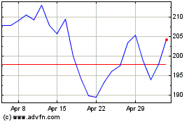
Applied Materials (NASDAQ:AMAT)
Historical Stock Chart
From Dec 2024 to Jan 2025

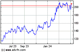
Applied Materials (NASDAQ:AMAT)
Historical Stock Chart
From Jan 2024 to Jan 2025
